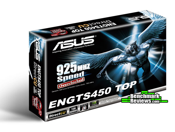
| ASUS ENGTS450 DirectCU TOP Video Card |
| Reviews - Featured Reviews: Video Cards | |||||||||||||||||||||||||||||||||||||||||||||||||||||||||||||||||||||||||||||||||||||||||||||||||||||||||||||||||||||||||||||||||||||||||||||||||||||||||||||||||||||||||||||||||||||||||||||||||||||||||||||||||||||||||||||||||||||||||||||||||||||||||||||||||||||||||||||||||||||||||||||||||||||||||||||||||||||||||||||||||||||||||||||||||||||||||||||||||||||||||||||||||||||||||||||||||||||||||||||||||||||||||||||||
| Written by Mathew Williams | |||||||||||||||||||||||||||||||||||||||||||||||||||||||||||||||||||||||||||||||||||||||||||||||||||||||||||||||||||||||||||||||||||||||||||||||||||||||||||||||||||||||||||||||||||||||||||||||||||||||||||||||||||||||||||||||||||||||||||||||||||||||||||||||||||||||||||||||||||||||||||||||||||||||||||||||||||||||||||||||||||||||||||||||||||||||||||||||||||||||||||||||||||||||||||||||||||||||||||||||||||||||||||||||
| Monday, 04 October 2010 | |||||||||||||||||||||||||||||||||||||||||||||||||||||||||||||||||||||||||||||||||||||||||||||||||||||||||||||||||||||||||||||||||||||||||||||||||||||||||||||||||||||||||||||||||||||||||||||||||||||||||||||||||||||||||||||||||||||||||||||||||||||||||||||||||||||||||||||||||||||||||||||||||||||||||||||||||||||||||||||||||||||||||||||||||||||||||||||||||||||||||||||||||||||||||||||||||||||||||||||||||||||||||||||||
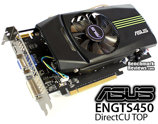
ASUS GeForce GTS 450 TOP Video Card ReviewLast month NVIDIA launched their new midrange video card: the GeForce GTS 450. Benchmark Reviews covered the launch with two articles focusing on single-card performance and SLI performance at reference clock speeds. In this review, we turn our attention to partner products. Specially, we take a look at an overclocked GTS 450 offered by ASUS. With a 925MHz core clock speed and DDR5 running at 4000MHz, the ENGTS450 DirectCU TOP ships out well above the reference clocks speeds we benchmarked at during the launch and represents ASUS' highest out-the-door overclock. In this review, we'll put it to the test against a similar clocked offering from EVGA, AMD's HD5770, and one of the previous generation's top cards: the HD4870. In addition to overclocking, ASUS includes a few other features with the ENGTS450 designed to offer increased performance and entice consumers. One of the most obvious is the non-reference heatsink and fan, termed DirectCU. As the name implies, the HSF utilizes copper heat pipes that make direct contact with the GPU. The power PCB itself is also non-reference and includes an upgraded four-phase power design. Mated with ASUS' Voltage Tweak, they claim up to 50% performance gains.
Manufacturer overclocking and extras are often accompanied by a price premium and the ASUS ENGTS450 is no exception. However, at only $10 more than reference cards, it promises to be great value. To find out just what that $10 gets you, we'll put the ENGTS450 through its paces in our benchmark suite. Up first, though, we take a look at the GF106 architecture and the card itself.
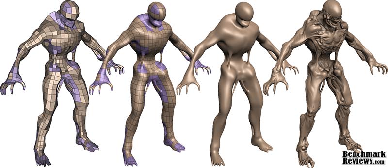
Manufacturer: ASUSTek Computer, Inc. Full Disclosure: The product sample used in this article has been provided by ASUS. NVIDIA Fermi FeaturesIn today's complex graphics, tessellation offers the means to store massive amounts of coarse geometry, with expand-on-demand functionality. In the NVIDIA GF104 GPU (GF100 series), tessellation also enables more complex animations. In terms of model scalability, dynamic Level of Detail (LOD) allows for quality and performance trade-offs whenever it can deliver better picture quality over performance without penalty. Comprised of three layers (original geometry, tessellation geometry, and displacement map), the final product is far more detailed in shade and data-expansion than if it were constructed with bump-map technology. In plain terms, tessellation gives the peaks and valleys with shadow detail in-between, while previous-generation technology (bump-mapping) would give the illusion of detail.
Stages of Tessellation with NVIDIA Fermi GraphicsUsing GPU-based tessellation, a game developer can send a compact geometric representation of an object or character and the tessellation unit can produce the correct geometric complexity for the specific scene. Consider the "Imp" character illustrated above. On the far left we see the initial quad mesh used to model the general outline of the figure; this representation is quite compact even when compared to typical game assets. The two middle images of the character are created by finely tessellating the description at the left. The result is a very smooth appearance, free of any of the faceting that resulted from limited geometry. Unfortunately this character, while smooth, is no more detailed than the coarse mesh. The final image on the right was created by applying a displacement map to the smoothly tessellated third character to the left. What's new in Fermi?With any new technology, consumers want to know what's new in the product. The goal of this article is to share in-depth information surrounding the Fermi architecture, as well as the new functionality unlocked in GF100. For clarity, the 'GF' letters used in the GF100 GPU name are not an abbreviation for 'GeForce'; they actually denote that this GPU is a Graphics solution based on the Fermi architecture. The next generation of NVIDIA GeForce-series desktop video cards will use the GF100 to promote the following new features:
Tessellation in DirectX-11Control hull shaders run DX11 pre-expansion routines, and operates explicitly in parallel across all points. Domain shaders run post-expansion operations on maps (u/v or x/y/z/w) and is also implicitly parallel. Fixed function tessellation is configured by Level of Detail (LOD) based on output from the control hull shader, and can also produce triangles and lines if requested. Tessellation is something that is new to NVIDIA GPUs, and was not part of GT200 because of geometry bandwidth bottlenecks from sequential rendering/execution semantics. In regard to the GF100-series graphics processor, NVIDIA has added a new PolyMorph and Raster engines to handle world-space processing (PolyMorph) and screen-space processing (Raster). There are eight PolyMorph engines and two Raster engines on the GF104, which depend on an improved L2 cache to keep buffered geometric data produced by the pipeline on-die. Four-Offset Gather4The texture unit on previous processor architectures operated at the core clock of the GPU. On GF104, the texture units run at a higher clock, leading to improved texturing performance for the same number of units. GF104's texture units now add support for DirectX-11's BC6H and BC7 texture compression formats, reducing the memory footprint of HDR textures and render targets. The texture units also support jittered sampling through DirectX-11's four-offset Gather4 feature, allowing four texels to be fetched from a 128×128 pixel grid with a single texture instruction. NVIDIA GF100 series GPUs implements DirectX-11 four-offset Gather4 in hardware, greatly accelerating shadow mapping, ambient occlusion, and post processing algorithms. With jittered sampling, games can implement smoother soft shadows or custom texture filters efficiently. The previous GT200 GPU did not offer coverage samples, while the GF100-series can deliver 32x CSAA. GF106 Compute for GamingAs developers continue to search for novel ways to improve their graphics engines, the GPU will need to excel at a diverse and growing set of graphics algorithms. Since these algorithms are executed via general compute APIs, a robust compute architecture is fundamental to a GPU's graphical capabilities. In essence, one can think of compute as the new programmable shader. GF100's compute architecture is designed to address a wider range of algorithms and to facilitate more pervasive use of the GPU for solving parallel problems. Many algorithms, such as ray tracing, physics, and AI, cannot exploit shared memory-program memory locality is only revealed at runtime. GF106's cache architecture was designed with these problems in mind. With up to 48 KB of L1 cache per Streaming Multiprocessor (SM) and a global L2 cache, threads that access the same memory locations at runtime automatically run faster, irrespective of the choice of algorithm. NVIDIA Codename NEXUS brings CPU and GPU code development together in Microsoft Visual Studio 2008 for a shared process timeline. NEXUS also introduces the first hardware-based shader debugger. NVIDIA GF100-series GPUs are the first to ever offer full C++ support, the programming language of choice among game developers. To ease the transition to GPU programming, NVIDIA developed Nexus, a Microsoft Visual Studio programming environment for the GPU. Together with new hardware features that provide better debugging support, developers will be able enjoy CPU-class application development on the GPU. The end results is C++ and Visual Studio integration that brings HPC users into the same platform of development. NVIDIA offers several paths to deliver compute functionality on the GF106 GPU, such as CUDA C++ for video games. Image processing, simulation, and hybrid rendering are three primary functions of GPU compute for gaming. Using NVIDIA GF100-series GPUs, interactive ray tracing becomes possible for the first time on a standard PC. Ray tracing performance on the NVIDIA GF100 is roughly 4x faster than it was on the GT200 GPU, according to NVIDIA tests. AI/path finding is a compute intensive process well suited for GPUs. The NVIDIA GF100 can handle AI obstacles approximately 3x better than on the GT200. Benefits from this improvement are faster collision avoidance and shortest path searches for higher-performance path finding. NVIDIA GigaThread Thread SchedulerOne of the most important technologies of the Fermi architecture is its two-level, distributed thread scheduler. At the chip level, a global work distribution engine schedules thread blocks to various SMs, while at the SM level, each warp scheduler distributes warps of 32 threads to its execution units. The first generation GigaThread engine introduced in G80 managed up to 12,288 threads in real-time. The Fermi architecture improves on this foundation by providing not only greater thread throughput, but dramatically faster context switching, concurrent kernel execution, and improved thread block scheduling. NVIDIA GF106 GPU Fermi ArchitectureBased on the Fermi architecture, NVIDIA's latest GPU is codenamed GF106 and is equipped on the GeForce GTS 450. In this article, Benchmark Reviews explains the technical architecture behind NVIDIA's GF106 graphics processor and offers an insight into upcoming Fermi-based GeForce video cards. For those who are not familiar, NVIDIA's GF100 GPU was their first graphics processor to support DirectX-11 hardware features such as tessellation and DirectCompute, while also adding heavy particle and turbulence effects. The GF100 GPU is also the successor to the GT200 graphics processor, which launched in the GeForce GTX 280 video card back in June 2008. NVIDIA has since redefined their focus, allowing subsequent GF100, GF104, and now GF106 GPUs to prove their dedication towards next generation gaming effects such as raytracing, order-independent transparency, and fluid simulations. While processor cores have grown from 128 (G80) and 240 (GT200), they reach 512 in the GF100 and earn the title of NVIDIA CUDA (Compute Unified Device Architecture) cores. GF100 was not another incremental GPU step-up like we had going from G80 to GT200. GF100 featured 512 CUDA cores, while GF104 was capable of 336 cores. Effectively cutting the eight SMUs on GF104 in half, NVIDIA's GF106 is good for 192 CUDA cores from four SMUs. The key here is not only the name, but that the name now implies an emphasis on something more than just graphics. Each Fermi CUDA processor core has a fully pipelined integer arithmetic logic unit (ALU) and floating point unit (FPU). GF106 implements the IEEE 754-2008 floating-point standard, providing the fused multiply-add (FMA) instruction for both single and double precision arithmetic. FMA improves over a multiply-add (MAD) instruction by doing the multiplication and addition with a single final rounding step, with no loss of precision in the addition. FMA minimizes rendering errors in closely overlapping triangles. GF106 implements 192 CUDA cores, organized as 8 SMs of 48 cores each. Each SM is a highly parallel multiprocessor supporting up to 32 warps at any given time (four Dispatch Units per SM deliver two dispatched instructions per warp for four total instructions per clock per SM). Each CUDA core is a unified processor core that executes vertex, pixel, geometry, and compute kernels. A unified L2 cache architecture (512KB on 1GB cards) services load, store, and texture operations. GF106 is designed to offer a total of 16 ROP units pixel blending, antialiasing, and atomic memory operations. The ROP units are organized in four groups of eight. Each group is serviced by a 64-bit memory controller. The memory controller, L2 cache, and ROP group are closely coupled-scaling one unit automatically scales the others.
Based on Fermi's third-generation Streaming Multiprocessor (SM) architecture, GF106 could be considered a divided GF104. NVIDIA GeForce GF100-series Fermi GPUs are based on a scalable array of Graphics Processing Clusters (GPCs), Streaming Multiprocessors (SMs), and memory controllers. NVIDIA's GF100 GPU implemented four GPCs, sixteen SMs, and six memory controllers. GF104 implements two GPCs, eight SMs, and four memory controllers. Conversely, GF106 houses one GPC, four SMs, and two memory controllers. Where each SM contained 32 CUDA cores in the GF100, NVIDIA configured GF104 with 48 cores per SM... which has been repeated for GF106. As expected, NVIDIA Fermi-series products are launching with different configurations of GPCs, SMs, and memory controllers to address different price points. CPU commands are read by the GPU via the Host Interface. The GigaThread Engine fetches the specified data from system memory and copies them to the frame buffer. GF106 implements two 64-bit GDDR5 memory controllers (128-bit total) to facilitate high bandwidth access to the frame buffer. The GigaThread Engine then creates and dispatches thread blocks to various SMs. Individual SMs in turn schedules warps (groups of 48 threads) to CUDA cores and other execution units. The GigaThread Engine also redistributes work to the SMs when work expansion occurs in the graphics pipeline, such as after the tessellation and rasterization stages. GF106 Specifications
GeForce 400-Series Specifications
Closer Look: ASUS GTS 450 DirectCU TOPAs I mentioned in the intro, the ASUS ENGTS450 DirectCU TOP includes a number of non-reference features as well as the standard items you'd expect from a mid-range video card. We'll first take a look at the overall appearance of the card, the video ports it offers, and the DirectCU heatsink and fan unit. Then, with the heatsink off, we'll move into some of the more technical details as we take a closer look at the chip itself, the memory, and the power circuitry.
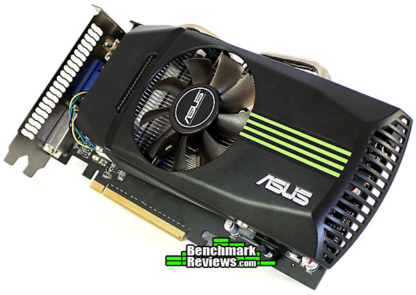
In the photo above, we get a good glimpse of the ENGTS450 as a whole. The fan and plastic shroud covering the heatsink are appropriately branded with the ASUS logo, but that's about as far as it goes--no full-length stickers or flashy graphics. I personally like the minimalist approach, but when graphics are done well, they look great as well. That said, I'm glad they went with a black PCB as it will match most of the motherboards out there. It's a bit hard to see in the photo, but they also include a metal bracket along the length of the PCB to provide additional rigidity and hold it level.
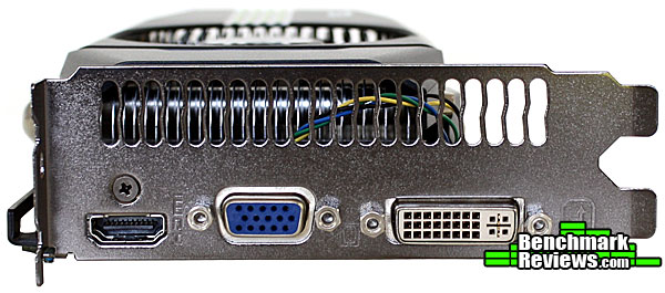
Turning out attention to the other side of the ENGTS450, we find the card's three display ports. HDMI, VGA, and DVI all come natively. I don't have much need for VGA these days, but there are those who may appreciate it. One thing definitely worth pointing out here, though, is the native HDMI support. The reference GTS 450 supports HDMI, but only has a mini connector. It's not a problem if you have a mini HDMI cable or the necessary adapter, but it's nice to have a full HDMI port built in. Of course, you give up the second DVI port to get it.
Another non-reference component is the heatsink and fan I mentioned earlier in the review. With it removed and cleaned off, it's clear why ASUS calls it DirectCU. Two copper heat pipes can be seen and are exposed directly to the GPU. ASUS claims that, as a result of this non-reference design, the entire heatsink and fan unit yields up to 20% lower temperatures during load and is up to 35% quieter while the card is idle. We won't be testing the sound level, but we will revisit the temperature claim a bit later in the review.
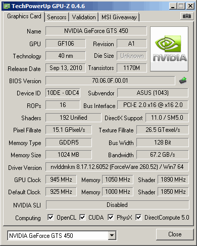
With the heatsink removed, we got our first look at the GF106 chip itself. The NVIDIA logo and a few other markings that got washed out in the light, but you can clearly see the die labeled with GF106-250-KA-A1. We discussed the architecture of the chip in detail on the previous page, so I won't go into detail here. What I do want to point out, though, are the clock speeds of our ENGTS450 TOP. The reference chip comes in at 783 MHz for the graphics clock and 1566 MHz for the CUDA cores. The ASUS card, on the other hand, manages 925 MHz and 1850 MHz, an 18% increase over stock--not bad for an extra $10.
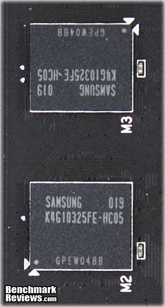
So far, we haven't discussed the memory in much detail. As you can see, the chips are from Samsung, part number K4G10325FE-HC05. Each chip is 128MB and our card has eight for a total of 1024MB. The same chips can be found on the on the reference model, which runs them at 3608MHz. However, they're actually rated for 4000MHz, which what ASUS decided to set them at with the ENGTS450 TOP.
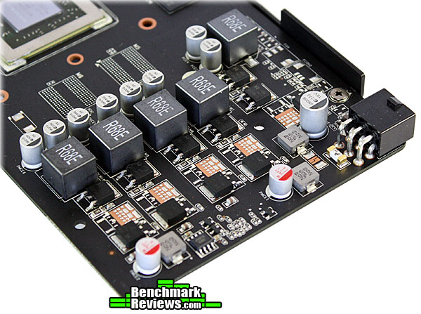
The last area where ASUS decided to up the ante is in the ENGTS450's VRM design. As you can see in the image above, they went with a four-phase approach and POSCAP capacitors (not pictured) to ensure adequate and stable voltage for overclocking. The voltage can be adjusted via ASUS' Smart Doctor software. With this Voltage Tweak technology, they claim that the consumer can achieve up to 50% faster performance. We'll, of course, put this claim to the test in our overclocking section. VGA Testing MethodologyThe Microsoft DirectX-11 graphics API is native to the Microsoft Windows 7 Operating System, and will be the primary O/S for our test platform. DX11 is also available as a Microsoft Update for the Windows Vista O/S, so our test results apply to both versions of the Operating System. The majority of benchmark tests used in this article are comparative to DX11 performance, however some high-demand DX10 tests have also been included.
According to the Steam Hardware Survey published for the month ending May 2010, the most popular gaming resolution is 1280x1024 (17-19" standard LCD monitors). Our benchmark performance tests typically concentrate the more demanding 1680x1050 (22-24" widescreen LCD) and 2.30MP 1920x1200 (24-28" widescreen LCD monitors) resolutions. However, as this is a mid-range video card, we've dropped the 1920x1200 benchmarks and added 1280x1024 to better capture the intended use of this card. In each benchmark test there is one 'cache run' that is conducted, followed by five recorded test runs. Results are collected at each setting with the highest and lowest results discarded. The remaining three results are averaged, and displayed in the performance charts on the following pages. A combination of synthetic and video game benchmark tests have been used in this article to illustrate relative performance among graphics solutions. Our benchmark frame rate results are not intended to represent real-world graphics performance, as this experience would change based on supporting hardware and the perception of individuals playing the video game. DX11 Cost to Performance RatioFor this article Benchmark Reviews has included cost per FPS for graphics performance results. Only the least expensive product price is calculated, and does not consider tax, freight, promotional offers, or rebates into the cost. All prices reflect product series components, and do not represent any specific manufacturer, model, or brand. These retail prices for each product were obtained from NewEgg.com on 30-September-2010:
AMD Phenom II Test System
DirectX-10 Benchmark Applications
DirectX-11 Benchmark Applications
Video Card Test Products
DX10: 3DMark Vantage3DMark Vantage is a PC benchmark suite designed to test the DirectX10 graphics card performance. FutureMark 3DMark Vantage is the latest addition the 3DMark benchmark series built by FutureMark corporation. Although 3DMark Vantage requires NVIDIA PhysX to be installed for program operation, only the CPU/Physics test relies on this technology. 3DMark Vantage offers benchmark tests focusing on GPU, CPU, and Physics performance. Benchmark Reviews uses the two GPU-specific tests for grading video card performance: Jane Nash and New Calico. These tests isolate graphical performance, and remove processor dependence from the benchmark results. 3DMark Vantage GPU Test: Jane NashOf the two GPU tests 3DMark Vantage offers, the Jane Nash performance benchmark is slightly less demanding. In a short video scene the special agent escapes a secret lair by water, nearly losing her shirt in the process. Benchmark Reviews tests this DirectX-10 scene at 1280x1024 and 1680x1050 resolutions, and uses Extreme quality settings with 8x anti-aliasing and 16x anisotropic filtering. The 1:2 scale is utilized, and is the highest this test allows. By maximizing the processing levels of this test, the scene creates the highest level of graphical demand possible and sorts the strong from the weak.
Cost Analysis: Jane Nash (1680x1050)3DMark Vantage GPU Test: New CalicoNew Calico is the second GPU test in the 3DMark Vantage test suite. Of the two GPU tests, New Calico is the most demanding. In a short video scene featuring a galactic battleground, there is a massive display of busy objects across the screen. Benchmark Reviews tests this DirectX-10 scene at 1280x1024 and 1680x1050 resolutions, and uses Extreme quality settings with 8x anti-aliasing and 16x anisotropic filtering. The 1:2 scale is utilized, and is the highest this test allows. Using the highest graphics processing level available allows our test products to separate themselves and stand out (if possible).
Cost Analysis: New Calico (1680x1050)Test Summary: Before we get into the numbers, I'd like to highlight the fact that we pitted three overclocked cards against a HD5770 running at reference speeds. It just happened to be what I had on hand, but it's something I will take into consideration throughout the review. If you're interested seeing how the reference GTS 450 performs, be sure to check out our GTS 450 launch article and the corresponding SLI analysis. That said, let's look at the results. In the Jane Nash benchmark, all four cards appear to hold their own, with the HD 4870 dropping slightly behind the newer generation cards. However, the New Calico benchmark tells a different story. The GTS 450's have roughly a 20-25% lead over the HD4870 and HD5770, which battle it out for last place. I'm not prepared to draw any conclusions after just one benchmark, but so far things are looking pretty good for the GTS 450.
DX10: Resident Evil 5Built upon an advanced version of Capcom's proprietary MT Framework game engine to deliver DirectX-10 graphic detail, Resident Evil 5 offers gamers non-stop action similar to Devil May Cry 4, Lost Planet, and Dead Rising. The MT Framework is an exclusive seventh generation game engine built to be used with games developed for the PlayStation 3 and Xbox 360, and PC ports. MT stands for "Multi-Thread", "Meta Tools" and "Multi-Target". Games using the MT Framework are originally developed on the PC and then ported to the other two console platforms. On the PC version of Resident Evil 5, both DirectX 9 and DirectX-10 modes are available for Microsoft Windows XP and Vista Operating Systems. Microsoft Windows 7 will play Resident Evil with backwards compatible Direct3D APIs. Resident Evil 5 is branded with the NVIDIA The Way It's Meant to be Played (TWIMTBP) logo, and receives NVIDIA GeForce 3D Vision functionality enhancements. NVIDIA and Capcom offer the Resident Evil 5 benchmark demo for free download from their website, and Benchmark Reviews encourages visitors to compare their own results to ours. Because the Capcom MT Framework game engine is very well optimized and produces high frame rates, Benchmark Reviews uses the DirectX-10 version of the test at 1280x1024 and 1680x1050 resolutions. Super-High quality settings are configured, with 8x MSAA post processing effects for maximum demand on the GPU. Results from the Scene #4 test are collected for the chart illustrated below.
Cost Analysis: Resident Evil 5 (Area 4)Test Summary: The Resident Evil benchmark really turns things upside down, with the older HD4870 taking the lead. My guess would be that is the 256-bit memory interface showing its strength. The other three cards have more processing power, but are limited by 128-bit memory interface. The other three cards are left to fight it out for second place and are fairly well matched.
DX11: Aliens vs PredatorAliens vs. Predator is a science fiction first-person shooter video game, developed by Rebellion, and published by Sega for Microsoft Windows, Sony PlayStation 3, and Microsoft Xbox 360. Aliens vs. Predator utilizes Rebellion's proprietary Asura game engine, which had previously found its way into Call of Duty: World at War and Rogue Warrior. The self-contained benchmark tool is used for our DirectX-11 tests, which push the Asura game engine to its limit. In our benchmark tests, Aliens vs. Predator was configured to use the highest quality settings with 4x AA and 16x AF. DirectX-11 features such as Screen Space Ambient Occlusion (SSAO) and tessellation have also been included, along with advanced shadows.
Cost Analysis: Aliens vs Predator (1680x1050)Test Summary: Now that we're into the DirectX 11 benchmarks, the HD4870 is out and we focus in a bit more on the reference HD5770 versus our overclocked GTS 450 cards. All three cards perform well, but the GTS 450's do manage to pull ahead just a bit.
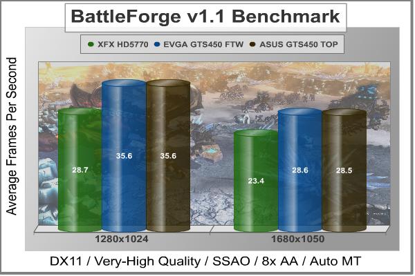
DX11: BattleForgeBattleForge is free Massive Multiplayer Online Role Playing Game (MMORPG) developed by EA Phenomic with DirectX-11 graphics capability. Combining strategic cooperative battles, the community of MMO games, and trading card gameplay, BattleForge players are free to put their creatures, spells and buildings into combination's they see fit. These units are represented in the form of digital cards from which you build your own unique army. With minimal resources and a custom tech tree to manage, the gameplay is unbelievably accessible and action-packed. Benchmark Reviews uses the built-in graphics benchmark to measure performance in BattleForge, using Very High quality settings (detail) and 8x anti-aliasing with auto multi-threading enabled. BattleForge is one of the first titles to take advantage of DirectX-11 in Windows 7, and offers a very robust color range throughout the busy battleground landscape. The charted results illustrate how performance measures-up between video cards when Screen Space Ambient Occlusion (SSAO) is enabled.
Cost Analysis: BattleForge (1680x1050)Test Summary: The overclocked GTS 450 cards are the clear winner when it comes to BattleForge. At 1280x1024 they maintain a 24% advantage over the HD5770 and at 1680x1050, a 22% advantage.
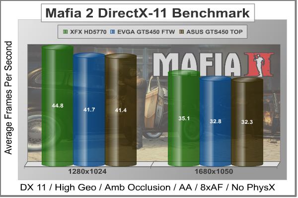
DX9+SSAO: Mafia IIMafia II is a single-player third-person action shooter developed by 2K Czech for 2K Games, and is the sequel to Mafia: The City of Lost Heaven released in 2002. Players assume the life of World War II veteran Vito Scaletta, the son of small Sicilian family who immigrates to Empire Bay. Growing up in the slums of Empire Bay teaches Vito about crime, and he's forced to join the Army in lieu of jail time. After sustaining wounds in the war, Vito returns home and quickly finds trouble as he again partners with his childhood friend and accomplice Joe Barbaro. Vito and Joe combine their passion for fame and riches to take on the city, and work their way to the top in Mafia II. Mafia II is a DirectX-9/10/11 compatible PC video game built on 2K Czech's proprietary Illusion game engine, which succeeds the LS3D game engine used in Mafia: The City of Lost Heaven. In our Mafia-II Video Game Performance article, Benchmark Reviews explored characters and gameplay while illustrating how well this game delivers APEX PhysX features on both ATI and NVIDIA products. Thanks to DirectX-11 APEX PhysX extensions that can be processed by the system's CPU, Mafia II offers gamers equal access to high-detail physics regardless of video card manufacturer. PhysX Disabled
Cost Analysis: Mafia II (1680x1050)Medium PhysX
Cost Analysis: Mafia II (1680x1050)Test Summary: The Mafia II benchmark offers a great opportunity to compare the effects of GPU-based and CPU-based PhysX. In the first benchmark, with PhysX disabled, the HD5770 manages a small, but observable lead over the GTS 450's. With medium PhysX enabled, however, that lead quickly and dramatically disappears as the HD5770 system cannot run the PhysX calculations on the GPU. I won't get into the open-vs-propriety physics debate here, but suffice it to say that GTS 450 will have a significant advantage over the HD5770 when PhysX is utilized.
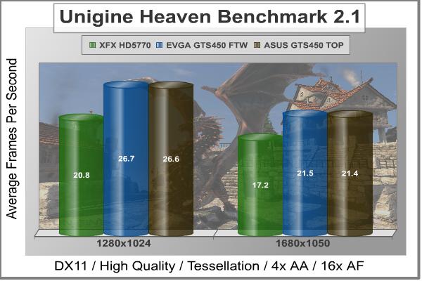
DX11: Unigine Heaven 2.1The Unigine "Heaven 2.1" benchmark is a free publicly available tool that grants the power to unleash the graphics capabilities in DirectX-11 for Windows 7 or updated Vista Operating Systems. It reveals the enchanting magic of floating islands with a tiny village hidden in the cloudy skies. With the interactive mode, emerging experience of exploring the intricate world is within reach. Through its advanced renderer, Unigine is one of the first to set precedence in showcasing the art assets with tessellation, bringing compelling visual finesse, utilizing the technology to the full extend and exhibiting the possibilities of enriching 3D gaming. The distinguishing feature in the Unigine Heaven benchmark is a hardware tessellation that is a scalable technology aimed for automatic subdivision of polygons into smaller and finer pieces, so that developers can gain a more detailed look of their games almost free of charge in terms of performance. Thanks to this procedure, the elaboration of the rendered image finally approaches the boundary of veridical visual perception: the virtual reality transcends conjured by your hand. The "Heaven" benchmark excels at providing the following key features:
Cost Analysis: Unigine Heaven (1680x1050)Test Summary: Unigine Heaven is another clear winner for the overclocked GTS 450 based cards. The 28% increase in the 1280x1024 run and 25% increase in the 1680x1050 run speak for themselves. Considering the overclock on these cards is roughly 18%, a reference GTS 450 would likely still come out slightly ahead of the HD5770. In fact, this is exactly what we found during our Unigine Heaven benchmarking last month.
ASUS ENGTS450 TOP TemperaturesBenchmark tests are always nice, so long as you care about comparing one product to another. But when you're an overclocker, gamer, or merely a PC hardware enthusiast who likes to tweak things on occasion, there's no substitute for good information. Benchmark Reviews has a very popular guide written on Overclocking Video Cards, which gives detailed instruction on how to tweak a graphics cards for better performance. Of course, not every video card has overclocking head room. Some products run so hot that they can't suffer any higher temperatures than they already do. This is why we measure the operating temperature of the video card products we test. To begin testing, we use GPU-Z to measure the temperature at idle as reported by the GPU. Next we use FurMark's "Torture Test" to generate maximum thermal load and record GPU temperatures at high-power 3D mode. The ambient room temperature remained at a stable 23°C throughout testing. FurMark does two things extremely well: drive the thermal output of any graphics processor higher than applications of video games realistically could, and it does so with consistency every time. Furmark works great for testing the stability of a GPU as the temperature rises to the highest possible output. The temperatures discussed below are absolute maximum values, and not representative of real-world performance.
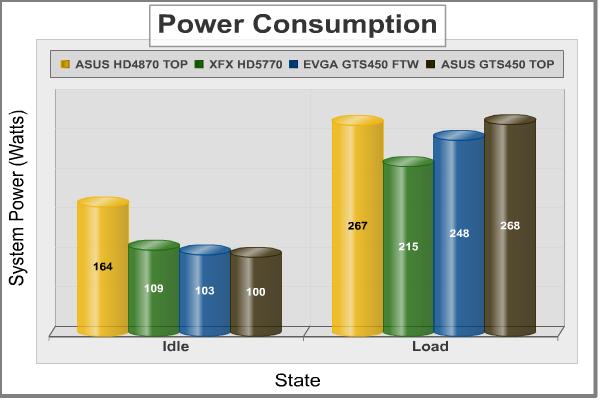
The two GTS 450 cards are fairly matched at idle, with the HD5770 coming in slightly warmer, and the HD4870 running considerably hotter. Once a load is applied, though, the heatsink and fan unit on the HD4870 show its strength. Of course, it was the loudest of the three as well. The HD5770 clearly runs the hottest, followed by the EVGA GTS450 FTW. Thanks to the DirectCU cooler we looked at earlier, though, the ASUS ENGTS450 TOP manages to keep itself a bit cooler. It's not quite the 20% ASUS claimed, but it's still decent and didn't result in any noticeable increase in noise over the EGVGA. VGA Power ConsumptionLife is not as affordable as it used to be, and items such as gasoline, natural gas, and electricity all top the list of resources which have exploded in price over the past few years. Add to this the limit of non-renewable resources compared to current demands, and you can see that the prices are only going to get worse. Planet Earth is needs our help, and needs it badly. With forests becoming barren of vegetation and snow capped poles quickly turning brown, the technology industry has a new attitude towards turning "green". I'll spare you the powerful marketing hype that gets sent from various manufacturers every day, and get right to the point: your computer hasn't been doing much to help save energy... at least up until now. A baseline test is taken with the system in an idle state. Once the baseline reading has been taken, the loaded power consumption reading is taken with the video card running a stress test using FurMark. Below is a chart with the total system power displayed in Watts for each specified test product:
Our power consumption tests tell a much different story than the temperatures. The HD4870 is clearly the power hog at idle, while the other three cards all sit within about 9% of each other. At load, however, the HD5770 consumes much less power than the other cards. What's interesting, though, is how much more energy the ASUS GTS 450 consumes over the EVGA model. Both are overclocked by a similar amount, by the higher core voltage of the ASUS card is definitely revealed in this test. While probably not the best for the environment, this may appeal to enthusiasts; a higher core voltage can often help achieve a better overclock, which we look at in the next section. ASUS ENGTS450 TOP OverclockingOverclocking the ASUS ENGTS450 TOP was a challenge. There wasn't much headroom left, which comes as no surprise considering this is the highest-clocked GTS 450 ASUS has put out. I did try increasing the voltage, made possible thanks to the upgraded VRM and Smart Doctor Software, but it didn't appear to have much effect. After several rounds of tweaking and stability testing, I settled on the speeds you see below.
At 945MHz, the GPU overclocked to roughly 2% higher than the stock speed for the ENGTS450 TOP and 21% higher than NVIDIA's reference design. The memory managed 4200MHz, a 5% increase over the ENGTS450 TOP and 16% over reference. I could have pushed it higher and still made it through the benchmarks, but at the cost of severe artifacting and possible damage over time. That said, here are the benchmark results of the stable clock speeds I was able to achieve:
With an average increase of only 3.4%, it's clear ASUS is already pushing this card fairly hard. Still, some will want those extra percent. Personally, though, I'd rather have the long-term stability of the stock overclock. Sure, you may never have a problem running at the higher speeds, but for such a small increase I'd rather stick with speeds that I know are going to hold up over time and are guaranteed by warranty. NVIDIA GTS 450 Final ThoughtsThe GTS is definitely a good move for NVIDIA. They really needed a current generation card that could compete in this price range. Looking at the benchmark results in this review, they clearly met this goal. Our two overclocked GTS 450's managed to outperform the Radeon HD5770 in the majority of the tests we ran. Of course, as I noted at the beginning of the benchmarks, the HD5770 we used ran at reference speeds. There are a number overclocked HD5770's on the market that could (feasibly) flip the scales back in favor of the HD5770. Where the GTS 450 really differentiates itself, though, is in price. Most GTS 450's are selling for $120 - $140, while the HD5770's are still in the $140 - $160 range. That gives the GTS 450 based cards a nice edge in terms of value. As we saw throughout the benchmarking sections, our GTS 450 cards consistently had a lower cost per fps.
With AMD set to launch its next series by the end of the year, though, NVIDIA would be wise make the most of this advantage while it lasts. It's not clear yet whether AMD will be launching a new card in this category right away, but when they do, NVIDIA will need to be ready to counter it. Let's hope they have something equally impressive up their sleeves. ASUS ENGTS450 TOP ConclusionThe ASUS ENGTS450 DirectCU TOP performed admirably in all of the benchmarks we threw at it. In most tests, it managed to pull ahead of the more expensive HD5770 and held its own against the comparably-clocked EVGA GTS 450 FTW. As I pointed out several time in the article, HD5770 was running at reference speeds and were it an overclocked version, the results may have been reversed. However, lower price of the ENGTS450 still gives it the advantage when looking at the price-performance ratio. While performance is undoubtably the top concern when it comes to video cards, appearance can often be a deciding factor between two comparable models. It's somewhat subjective, but in my opinion, the ENGTS450 does really well here. The black PCB is fairly neutral and should match most other components well. The heatsink and fan unit is well designed, displaying ASUS' branding without going too over the top with graphics and stickers. Full length stickers can look good, but can also look cheap if not done right. ASUS avoids this issue by going with a matte finish on the fan shroud. The only thing I would add is a sleeve for the fan wiring.
Construction quality tends to be another big tie-breaker when it comes to video cards. Other than good quality assurance testing, there's not much a partner like ASUS can do about the quality of the actual GPU chip. However, they did include a number of non-reference features that should help out with the durability and reliability of the card as a whole. The full-length metal bracket along the side adds additional rigidity and should help reduce problems related to PCB or GPU strain. One of the most important upgrades, though, is to the VRM. The four-phase design and POSCAPs should provide plenty clean, stable power to the GPU over its lifetime. ASUS' Smart Doctor software gives the consumer full control over the upgraded VRM. It can be used to change the voltage, as well as the core/shader clock speed and memory frequency. Keep in mind, though, that any increase in voltage will result in an increase in heat and power consumption. With the upgraded cooler, heat likely won't be a problem unless you're really pushing it. However, there's no avoiding the increased power consumption that accompanies higher voltages. As we saw in our overclocking section, though, pushing this card higher than the factory overclock is not really necessary and adds little benefit for most consumers. At $139.99, the stock configuration is already an incredible value. The ASUS ENGTS450 TOP outperformed our reference HD5770 and costs $10 less. With new product launches coming from AMD and (potentially) NVIDIA by the end of the year, though, the mainstream graphics war rages on. Pros:
|
|||||||||||||||||||||||||||||||||||||||||||||||||||||||||||||||||||||||||||||||||||||||||||||||||||||||||||||||||||||||||||||||||||||||||||||||||||||||||||||||||||||||||||||||||||||||||||||||||||||||||||||||||||||||||||||||||||||||||||||||||||||||||||||||||||||||||||||||||||||||||||||||||||||||||||||||||||||||||||||||||||||||||||||||||||||||||||||||||||||||||||||||||||||||||||||||||||||||||||||||||||||||||||||||


Comments
DX11: Mafia II ?????
/index.php?option=com_content&task=view&id=617&Itemid=72&limit=1&limitstart=9
i bought this version n i dunno what to setup for Vcore...
what is Vcore actually??
and can what happen if i slightly change the value of engine core?